- Solutions
- Capabilities
-
-
Design
-
Fabricate
-
Assemble & Test
-
QA
-
-
- Fabricated Parts
- Industries
- About
Get Engineering Help:(978) 538-0808
Silicon wafer marking is the process of applying unique identifying marks or patterns onto the surface of a silicon wafer.
Our core business philosophy centers around understanding your business and the products you offer in order to provide the best service possible. We take pride in our flexibility and commitment to meeting our customers’ needs, which is why we offer customized manufacturing plans tailored to your specific requirements.
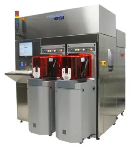
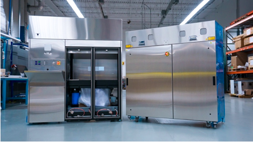
With our extensive experience in manufacturing semiconductor equipment, we recognize that the production process for silicon wafer marking equipment involves numerous intricate steps and processes. These tools are delicate and sensitive, and our customers rely on our expertise to create a refined manufacturing process that upholds the highest standards of quality.
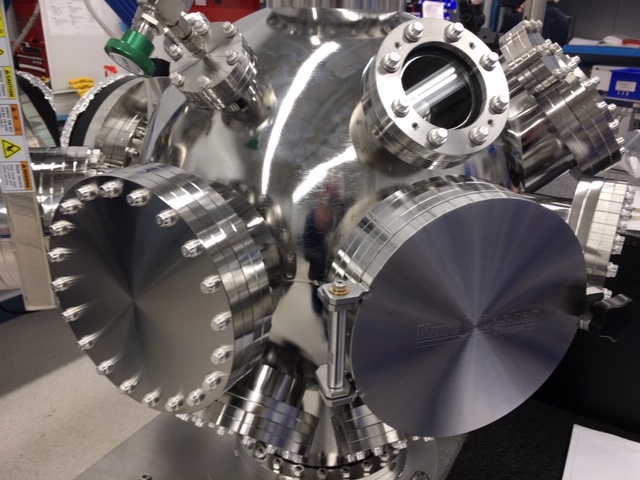
In this particular case, we reached a mutual agreement with our customer to focus on manufacturing the base unit of the wafer marking equipment. This includes the frame, structural and process-related fabricated components, electronics, and exterior panels. By adopting this approach, we can concentrate on the overall mechanical and electrical build, while enabling our customer the ability to retain control of their intellectual property and manage costs by procuring and installing key components during the final build and tool qualification at their facility.
Overall, silicon wafer marking plays a crucial role in the semiconductor manufacturing industry, providing identification, traceability, and data management capabilities that contribute to improved production efficiency, quality control, and yield optimization
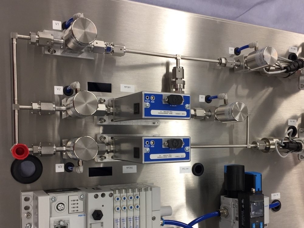
We assigned a dedicated engineer from the outset of our relationship, serving as a single point of contact. Supported by our entire organization, this engineer ensures an unparalleled level of service. As we are responsible for manufacturing only a portion of the wafer mark tool, our engineering team streamlined the bill of materials (BOM) and related documentation, focusing solely on the components we fabricate, (several internally) and procure.
Our manufacturing process incorporates robust quality control measures to ensure that the equipment meets the specified standards and performance requirements. Quality checks, inspections, and tests are conducted at various stages of the manufacturing process to identify and rectify any issues or defects. A comprehensive final quality checklist is used by our quality walk-around team, who also document every aspect of product integrity through detailed photos.
Our procurement team carefully sources various components required for the equipment, including fabricated (CNC) components (some of which are produced in-house), electronics, control systems, sensors and many others. We leverage our extensive supply chain and take advantage of EOQ (economic order quantity) pricing. We procure the material based on the exact specifications provided by the customer but are experts in recommending alternative parts when faced with issues relating to EOL, (end of life) or long lead.
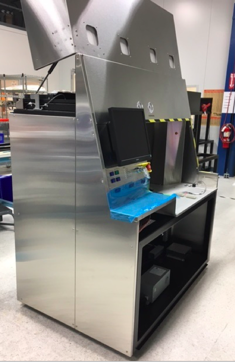
We have established flow lines and work cells to ensure efficient and consistent assembly of the wafer marking tools. Skilled technicians or assembly teams follow detailed instructions and guidelines provided by our customer, ensuring proper integration and alignment of the various parts to construct the wafer marking equipment precisely according to their specifications.
After assembly, the equipment undergoes rigorous testing. The equipment is tested to verify its functionality, accuracy, repeatability, and reliability. This process involves Hi-Pot testing, power-up and insuring that the emergency power off circuit and components are functioning to the customer prescribed specifications.
Our controlled environment, known as the White room, provides the necessary conditions to ensure cleanliness throughout the entire manufacturing process of the wafer mark tool. This cleanliness is essential as the equipment will be installed in a wafer fab where high levels of cleanliness are imperative.
To ensure safe transportation and delivery to our customers, the equipment is meticulously packaged with proper protection and labeling.
It is essential to emphasize that manufacturing silicon wafer marking equipment requires specialized knowledge, expertise, and dedicated facilities to guarantee the precision and reliability demanded by the semiconductor industry applications and more importantly, you as our valued customer.

By marking each wafer with a unique identifier, manufacturers can easily track and trace the wafer's progress during various stages of production. This helps ensure that the wafers are processed correctly and allows for quality control and process monitoring.
Marking wafers helps prevent mix-ups or confusion between different wafers during handling, processing, and testing. It ensures that wafers are correctly matched with their corresponding data, specifications, or manufacturing instructions.
The marking on the wafers helps in identifying individual wafers and their associated properties or characteristics. This information is useful for yield analysis, where manufacturers can identify and analyze patterns or trends in the performance or quality of wafers to improve overall production efficiency.
If a defect or issue arises during the manufacturing process, wafer marking assists in locating and isolating the problematic area. The marked pattern can act as a reference point for inspection, testing, or analysis, enabling manufacturers to pinpoint the precise location on the wafer that requires further investigation or correction.
Silicon wafer marking is the process of applying unique identifying marks or patterns onto the surface of a silicon wafer. Silicon wafers are thin, circular discs made of silicon that serve as the base material for manufacturing semiconductor devices such as integrated circuits (ICs) and microchips.
The purpose of silicon wafer marking is to enable traceability and identification throughout the semiconductor manufacturing process. Each silicon wafer is marked with a unique pattern, such as alphanumeric codes, barcodes, or logos, which can be read and interpreted by automated systems and humans.

Download this new guide and know the exact questions to ask as you review your vendors.
Download Now