- Solutions
- Capabilities
-
-
Design
-
Fabricate
-
Assemble & Test
-
QA
-
-
- Fabricated Parts
- Industries
- About
Get Engineering Help:(978) 538-0808

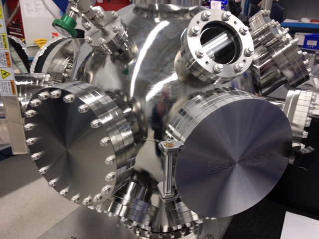
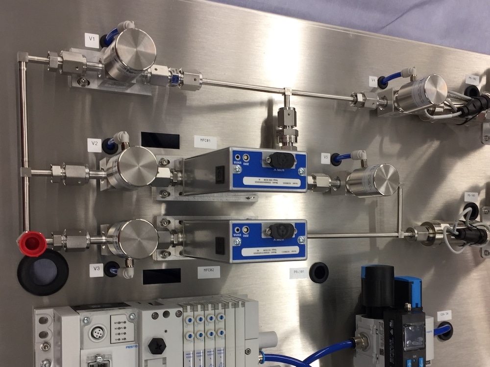
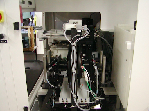
This local customer was in search of a local supplier that had the ability, primarily, to be able to provide engineering resources to work in collaboration with their engineering team. The objective was to refine the designs and define the manufacturing process for several different robotic and automated sub-assemblies of a much larger semiconductor tool. Additionally, the BOM’s contained a large number of precision machined components. Those components along with numerous commercial parts needed to be assembled and tested in a cleanroom. They recognized that by finding a competent supplier that could offer engineering services, precision machining and cleanroom assembly would free them up to direct their attention to the more complex IP issues of the much larger semiconductor processing tool. They quickly concluded that Innovent possessed the services they required all under one roof.
In the realm of semiconductor equipment manufacturing, the integration of robotics and automation has evolved to become a fundamental cornerstone of the industry. This transformation is driven by the industry’s pressing need for enhanced efficiency, precision, and reliability throughout the semiconductor fabrication process. These advanced technologies play a pivotal role in addressing the intricate challenges that arise when handling delicate silicon wafers and other critical components at high speeds, all while safeguarding these fragile materials from any form of damage. As the semiconductor value chain continues to diversify, with variable wafer sizes and demanding purity standards, the role of robots in this field has grown in complexity and importance. From ensuring cleanliness in controlled environments to delivering ultra-high precision and customized solutions, these robotic systems are indispensable for sustaining a safe, impurity-free workflow in semiconductor equipment manufacturing.
Robots are widely used in the semiconductor equipment manufacturing industry to handle silicon wafers with speed and precision. These robots are equipped with advanced sensors and software to ensure that the delicate wafers are transported without any damage. Variable wafer sizes and thicknesses pose a challenge, but specialized robots are capable of adapting to these variations.
Semiconductor fabrication demands an extremely clean and pure environment to prevent contamination that could affect the performance of the final components. Automated equipment and robots are designed to operate in cleanroom environments, ensuring that the manufacturing process remains free of impurities. Clean robots are equipped with features to minimize particle generation and to work in controlled environments.
The design of these robots is highly task specific. For instance, there are robots designed for inspection and cleaning, which require precise, controlled movements to maintain the cleanliness and quality of the wafers. Others are designed for front-end tasks like wafer orientation, which involves processes such as alignment and stacking.
For sensitive applications, cleanroom robot arms are employed. These robots are engineered to provide ultra-high performance, featuring smooth motion trajectories, high-speed operation, and exceptional accuracy. They can handle various semiconductor components like cassettes, silicon wafers, photomasks, and panels with the utmost precision.
Automation in semiconductor equipment manufacturing not only improves the precision of handling but also enhances overall workflow efficiency. These robots can work round the clock, reducing human labor and the risk of errors.
The use of robots also helps in quality assurance. The consistency and precision of robotic operations lead to a reduction in defects and wastage, ultimately contributing to cost-effectiveness.
In summary, robotics and automation are essential in semiconductor equipment manufacturing to meet the industry’s stringent requirements for purity, precision, and speed. Customized robots and equipment play a pivotal role in ensuring that semiconductor fabrication processes are carried out with the highest level of accuracy and cleanliness.
Your one-stop shop for complete fabrication, machining, welding and clean room assembly to exceed your project needs.
Download The Capabilities OverviewYou have challenges, and we certainly understand that. Put our expert engineers to work on YOUR projects and challenges.
Tell Us About Your Project & Make Manufacturing Easy
Download this new guide and know the exact questions to ask as you review your vendors.
Download Now