- Solutions
- Capabilities
-
-
Design
-
Fabricate
-
Assemble & Test
-
QA
-
-
- Fabricated Parts
- Industries
- About
Get Engineering Help:(978) 538-0808
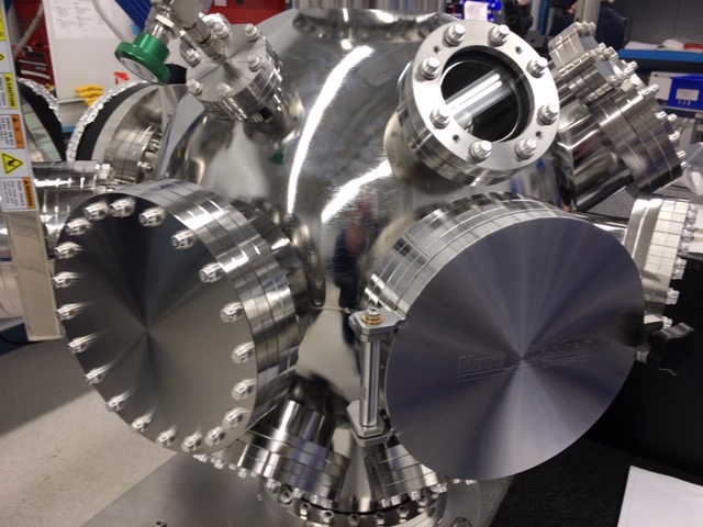
At Innovent we specialize in engineering and manufacturing solutions, particularly in the semiconductor industry. Our expertise lies in laser-driven light sources used for metrology and wafer inspection processes in semiconductor manufacturing although the manufacturing process is similar for all applications.
The use of optics but more specifically referred to as laser-driven light sources in metrology tools enables precise measurement and characterization of various parameters during the semiconductor manufacturing process. Interferometry techniques, scatterometry, and ellipsometry systems, among others, rely on lasers for accurate measurements of wafer thickness, surface roughness, film thickness, and critical dimensions. The coherent and focused nature of laser light allows for high precision and control in these measurements, ensuring the production of high-quality electronic components.
Wafer inspection systems that utilize laser-scanning or laser-based imaging techniques can detect defects or irregularities on semiconductor wafers. These laser-based detection systems are capable of identifying microscopic defects such as cracks, particles, or structural abnormalities, ensuring the overall quality of the semiconductor components.
This was a very important reason why this customer approached us to manufacture their products. As semiconductor features continue to shrink, the need for a sterile environment becomes essential to ensure the production of defect-free components.
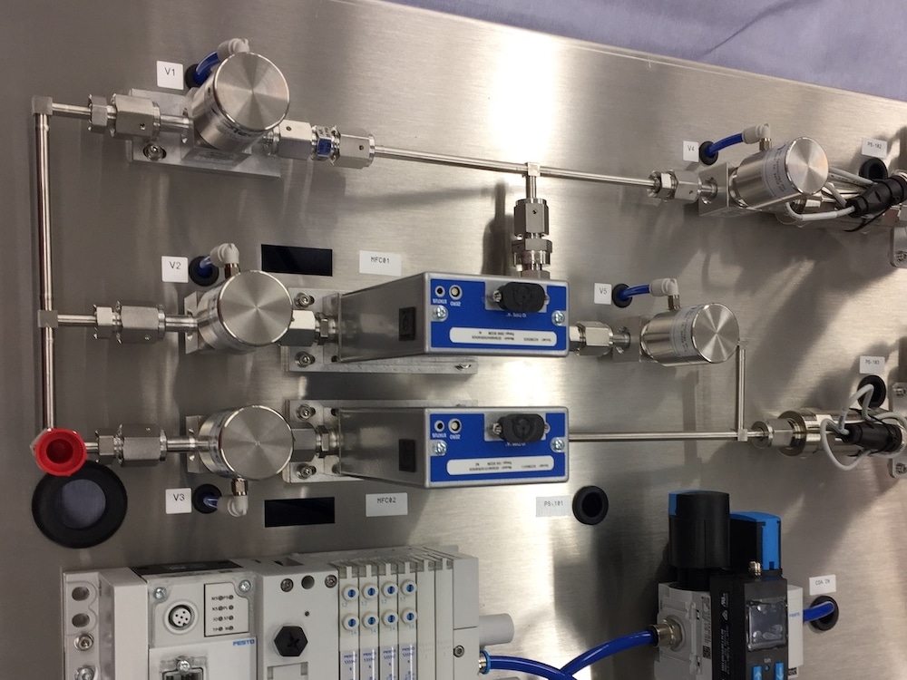
We met with the customer on several occasions and went through a very thorough interview process. Once the decision was made, we assigned an Engineering Customer Rep who would handle all aspects of the on-boarding process, which is our typical method of doing business. The manufacturing ramp-up was a collaborative process starting with co-builds and the product validation process. Once the customer was confident in our ability to perform those operations, we turned our attention to the value-add prospect of fabricating the key precision machined component which, in this case, resided with a supplier the customer was quite content with regarding cost and quality. This component, although relatively small in size, had hundreds of dimensions and an abundance of very tight GD&T callouts. We made it our mission to open a design & development project in order to win this aspect of the business.
This winning formula for our customer was precision machined component matched pricing, improved overall lead-time, a collaborative effort in ramping up Innovent to be the turn-key supplier for that product line and most importantly, much less time spent by our customer having to manage multiple suppliers.
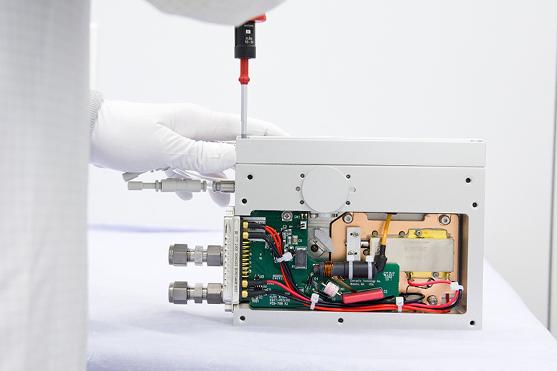
The final products are tested, packaged to SEMI standards, and delivered to the customer’s facility. The customer performs final assembly and product validation in their own cleanroom, maintaining control over their intellectual property (IP).
The Engineering Customer Rep serves as the main point of contact for day-to-day interactions throughout the entire relationship. He/she is backed by the support of the entire Innovent organization. Quarterly reviews are conducted to discuss various topics, including business overview, quality, on-time delivery data, supplier performance, and product yield.
This customer arrangement is described as typical for us, where we remain flexible and offer specialized services to customers while allowing them to retain control over their IP. This approach has proven to be successful in addressing the customer’s manufacturing challenges, leading them to continue leveraging Innovent’s services.
Laser-driven light sources refer to devices or systems that use lasers as the primary means to generate intense and coherent light. These sources harness the unique properties of lasers to produce light with specific characteristics, such as high brightness, narrow spectral linewidth, and high coherence.
Semiconductor lasers or laser diodes are compact and efficient light sources that emit coherent light through stimulated emission in a semiconductor material. They are commonly used in applications such as telecommunications, barcode readers, laser pointers, and optical storage devices.
These lasers use gas-filled tubes as the active medium to generate light. Examples include helium-neon (HeNe) lasers, argon-ion lasers, carbon dioxide (CO2) lasers, and excimer lasers. Gas lasers are widely used in scientific research, medical applications, laser light shows, and industrial processes.
Solid-state lasers utilize a solid material, such as a crystal or glass doped with rare-earth ions, as the gain medium. Examples include Nd:YAG (neodymium-doped yttrium aluminum garnet) lasers, ruby lasers, and titanium-sapphire lasers. Solid-state lasers are used in various fields, including medicine, material processing, laser marking, and research.
These lasers use laser diodes to pump a solid-state gain medium, typically a crystal or semiconductor. The diode-pumped lasers offer higher efficiency, compactness, and versatility compared to traditional lamp-pumped solid-state lasers. Examples include diode-pumped solid-state (DPSS) lasers and vertical-cavity surface-emitting lasers (VCSELs).
FELs are powerful light sources that use relativistic electron beams to generate coherent light across a wide range of wavelengths, from microwaves to X-rays. FELs are utilized in scientific research, such as studying atomic and molecular structure, materials science, and imaging techniques.
The choice of a specific light source depends on the desired characteristics, wavelength range, power requirements, and application in question. Laser technology continues to evolve, leading to advancements in light sources for various fields, including research, industry, telecommunications, and medicine.
Laser-driven light sources are extensively employed in photolithography, a key process in semiconductor manufacturing. High-power ultraviolet (UV) lasers, such as excimer lasers or solid-state lasers with harmonic generation, are used to expose and pattern photoresist materials on silicon wafers. These lasers provide the precise and intense light required to create intricate patterns and transfer them onto the semiconductor substrate.
In semiconductor fabrication, laser-driven light sources are employed for doping and annealing processes. Doping involves introducing impurities into the semiconductor material to alter its electrical properties. Laser beams can selectively heat localized regions of the wafer, facilitating the diffusion of dopant atoms. Similarly, laser annealing involves using high-energy laser pulses to melt and rapidly solidify specific areas of the semiconductor, resulting in improved crystalline structure and enhanced performance.
Laser-driven light sources find applications in micromachining processes, where precise material removal or modification is required. High-power lasers, such as femtosecond or picosecond lasers, can be used to ablate or etch semiconductor materials with exceptional precision. This enables the creation of microstructures, drilling of holes, or the removal of unwanted material layers in semiconductor devices.

Download this new guide and know the exact questions to ask as you review your vendors.
Download Now